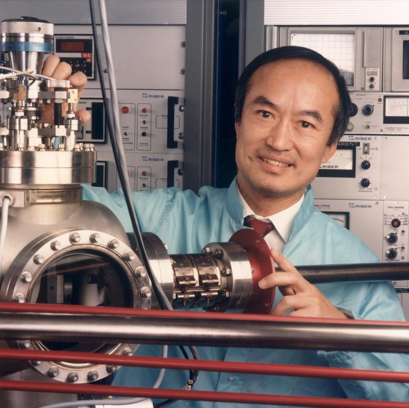
Molecular beam epitaxy, or MBE, is the process of growing high-purity crystals one atomic layer at a time. This allows engineers to create highly precise materials for a number of advanced electronics. If you have used a microwave oven, watched a DVD, listened to a CD, made a call on your cell phone, or you are reading these words on a computer, you have taken advantage of molecular beam epitaxy. And, for that, you have Alfred Y. Cho to thank.
If not for a warning from his mother, Cho nearly studied art instead of becoming a pioneer in engineering. “If you major in art, you’ll be very hungry,” she said, urging him to study medicine. Queasy around blood, Cho then looked to his siblings for inspiration. His older brother had decided to study mechanical engineering, Cho later recalled, and his older sister had picked architecture. “‘What’s left? What can I pick?’” Cho said he asked himself. “So that’s how I ended up with my field of electric engineering.”
By Jake New


